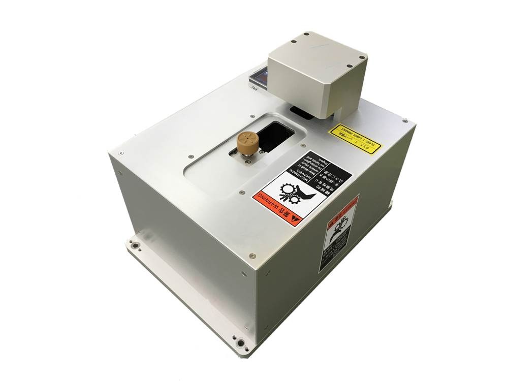


Features
- High speeds enabled by the units ability to center wafers and perform angle alignment without seperate chucking.
- Compatible with multiple wafers:50.8-100mm SEMI/JEIDA silicon wafers.
- Wafer size and nocth/flat are automatically recongnize,eliminating the need for host controller settings.
- Built-in controller for a compact design.
- Controllable through RS-232C or RS-485 serial interface or through photo I/O parallel communications.
- Configurable for compound semiconductor wafers and transparent glass wafers by utilizing CCD photo receiver for line sensor.
Specifications
| Handling object |
φ50.8mm to φ100mm SEMI/JEIDA standard wafer. (Please inquire with regard to special wafers such as glass wafers.) |
| Alignment time |
9.0seconds or less (When Processing φ100mm) |
| Alignment accuracy |
XY:±0.2mm or less(3σ) θ:±0.2° or less(3σ) |
| Wafer off-center limit |
±4mm or less (Wafer offset from chuck center) |
| Wafer holding method | Backside vacuum chuck |
| Wafer hold check | Vacuum sensor with digital display |
| Communication |
RS-232C,RS-485(Serial Interface) Photo I/O(Parallel interface) |
| Utility |
Power:DC24V±10% 5A 1line Vacuum:-80kPa or less.1line |
| Mass | Main body:Appox.12kg |
Contact us for questions about products.