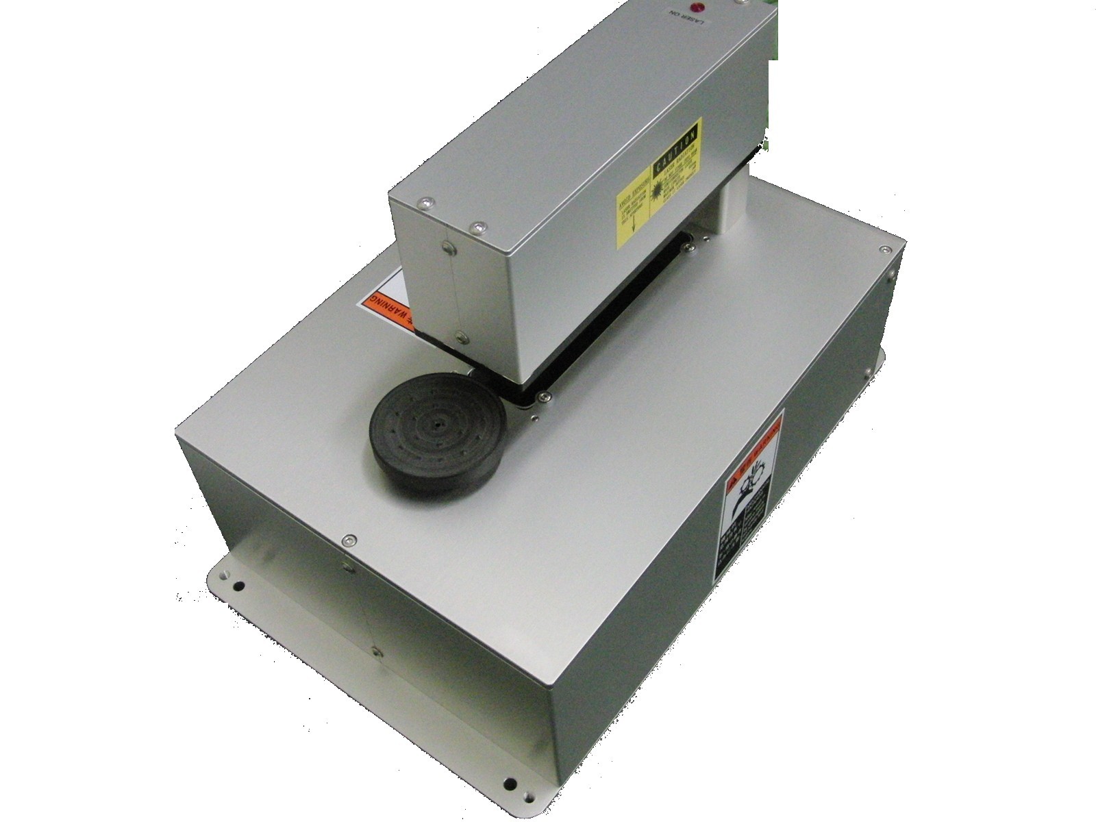
TA300A-VBD
This aligner enables to detect a wafer position by using a built-in sensor and to align a notch or orientation flat.
For centering of VA type, the additional mechanism(Robot etc) to execute a motion correction based on the data output from an aligner will be required.


Features
- Originally developed lader sensor enables to detect it regaedless of materials of wafer.
- The wafer size of 200mm to 300mm are automatically discriminated.
- Compact design realized a built-in controller.
- Guaranteed for three(3) years by high reliability design.
Specifications
| Handling object |
φ200mm to φ300mm SEMI/JEIDA standard wafer. (Please inquire with regard to special wafers such as glass wafers.) |
| Alignment time |
2.5seconds or less |
| Alignment accuracy |
XY:±0.1mm or less(3σ) θ:±0.1° or less(3σ) |
| Wafer off-center limit |
±5mm or less (Wafer offset from chuck center) |
| Wafer holding method | Backside vacuum chuck |
| Wafer hold check | Pressure sensor |
| Communication |
RS-232C(Serial Interface) |
| Utility |
Power:DC24V±10% 2A 1line Vacuum:φ6mm -80kPa or less 15L/min.1line |
| Mass | Main body:Appox.5kg |
Contact us for questions about products.