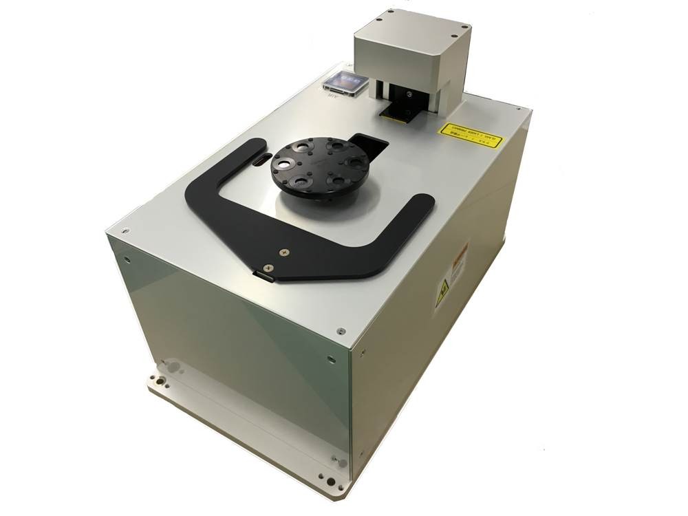


Features
- Thin wafer or warpsd wafer can be aligned by Bernoulli effect.
- Contact type is capable to handle as thin as 50μm thick wafers.
Specifications
| Handling object |
φ200mm to φ300mm SEMI/JEIDA standard wafer. (Please inquire with regard to special wafers such as glass wafers.) |
| Alignment time |
4.5seconds or less (When Processing φ300mm) |
| Alignment accuracy |
XY:±0.1mm or less(3σ) θ:±0.1° or less(3σ) |
| Wafer off-center limit |
±10mm or less (Wafer offset from chuck center) |
| Wafer holding method | Wafer Backside minimum partial contact |
| Wafer hold check | Reflective origin sensor |
| Communication |
RS-232C(Serial Interface) Photo I/O(Parallel interface) |
| Utility |
Power:DC24V±10% 5A 1line Dry air1:φ6mm 0.05 to 0.35MPa 100L/min,1line Dry air2:φ4mm 0.2 to 0.3MPa 100L/min,1line |
| Mass | Main body:Appox.14kg |
Contact us for questions about products.